The Process of Assembling a Flexible Printed Circuit Board
Assembling a Flexible Printed Circuit Board
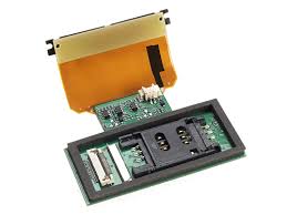
Flexible printed circuit boards (PCBs) are designed for dynamic applications like cell phones that need to bend in their pocket. They use a base material and solder mask that can flex with the circuit. A flex PCB can be manufactured with one, two, four, or more layers. The number of layers depends on the design and how much flexing it will need to do. Regardless of how many layers it has, it’s essential to have proper fabrication and assembly techniques so that the board will not fail in its intended usage.
The first step in a flexible printed circuit board fabrication is to prepare the base materials and the copper foil. A base material is an insulating layer that holds all of the components and connections together. The most common base material is polyimide, which offers greater flexibility and resistance to temperature fluctuations than epoxy resins. A copper foil is a conductive material that sits on top of the base material.
Next, the etching process is used to remove copper from the exposed surface of the PCB, leaving behind a patterned trace. This is done using a chemical called ferric chloride. The etched surface is then cover coated with a thin protective sheet known as a “coverlay.” The coverlay is cut to match the outline of the PCB drawing and then exposed to ultraviolet light, which hardens the coating.
The Process of Assembling a Flexible Printed Circuit Board
When the etching and covercoat processes are complete, it’s time to start assembling the flex PCB. The first step in flex PCB assembly is to check for component placement defects and dimensional accuracy. This can be done by visual inspection, X-ray, or automated test equipment. Next, the through hole components are soldered onto the traces and pads of the PCB. For this, it is important to have a reflow profile optimized for the specific flex materials being used. The use of these profiles can help minimize warpage and distortion in the finished product.
Lastly, any excess component leads that are sticking out of the bottom of the board should be trimmed with a cutting tool. This can prevent shorts during assembly. During this phase, it’s also critical to follow ESD control procedures as flex materials are more prone to static discharge damage.
Once the soldering is complete, the flex PCB is inspected for any imperfections or other issues that could affect its performance. The flex PCB can then be packaged for shipment. During packaging, the flex PCB must be securely wrapped and protected from shock and vibration, which can cause damage to components, solder joints, and the overall structure. This is why it’s so important to work with a reputable manufacturer that has the proper equipment and inspection techniques for flex manufacturing. They can ensure that your product will perform reliably in its intended environment, and provide you with high-quality results that meet industry standards.